Micro-Leads Plus Wettable Flanks: MLPAK Lets LFPAK Users Switch to the 12-Inch Platform Painlessly
Traditional automotive power devices have long faced a dilemma: leadless packages are compact, but solder joints crack easily and are hard to inspect with AOI; traditional leaded packages are reliable, but lack power density. Nexperia China's in-house MLPAK micro-lead package uses an innovative structure combining micro-leads with wettable flanks, keeping solder coverage above 80% after temperature cycling and delivering both mechanical reliability and process inspectability.
The full MLPAK range has passed AEC-Q101 automotive certification, covering both 3×3 and 5×6 mm sizes for applications at different power levels. More importantly, MLPAK is fully compatible with LFPAK PCB footprints, so customers can make a zero-cost replacement without changing their board design, greatly lowering the barrier to upgrading.
Nexperia China's proprietary 12-inch SGT T2X automotive MOSFETs are industry-leading on key metrics such as conduction loss, thermal performance, and surge withstand capability, filling the gap in 12-inch automotive-grade high-voltage MOSFETs.
According to industry information, the effective chip output of a single 12-inch wafer is about 5.7 times that of a 5-inch wafer, about 4 times that of a 6-inch wafer, and about 2.2 to 2.4 times that of an 8-inch wafer. In terms of per-chip cost, this means a reduction of about 70% compared with 5-inch, about 60% compared with 6-inch, and about 50% compared with 8-inch.
Development efficiency is equally striking. Nexperia's product development cycle used to take 24 to 36 months; now new product development takes 6 to 12 months. The localization ratio of some core devices has risen from under 20% to nearly 100%.
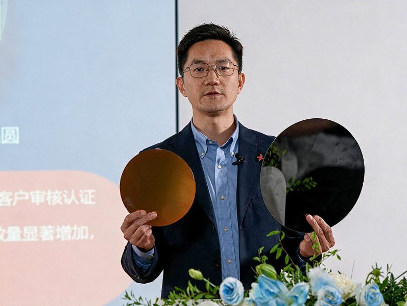
At the August 23 launch event, MLPAK appeared alongside the T2X platform and the 12-inch production line, becoming one of the main points of interest. For automakers and Tier-1 suppliers, it means a new automotive power device option with a better cost structure and steadier supply.
About Nexperia Semiconductors (China) Ltd.:
As a frontrunner in the development and production of basic semiconductor devices, Nexperia Semiconductors (China) Ltd. (Anshi China) offers devices that are widely used in various applications such as automotive, industrial, mobile, and consumer electronics, supporting almost all basic functions of electronic design worldwide. Nexperia Semiconductors (China) Ltd. (Anshi China) provides products and services to customers globally, with these products becoming industry benchmarks in terms of efficiency (such as process, size, power, and performance) and gaining widespread recognition. Nexperia Semiconductors (China) Ltd. (Anshi China) boasts a rich IP product portfolio and a continuously expanding product range, and has obtained certifications under the IATF16949, ISO9001, ISO14001, and ISO45001 standards, fully demonstrating the company's firm commitment to innovation, efficiency, sustainable development, and meeting stringent industry requirements.


.jpg)